


Description
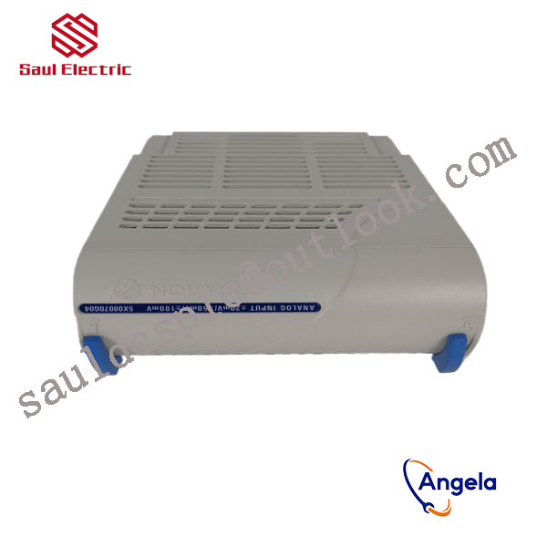
5X00070G05 Relay output logic module Emerson
thereby controlling external devices or circuits.
The receiver can adopt a larger number of digital integrated circuits. Of course, the closer the digital circuit of the receiver is to the antenna, the more it can leverage the advantages of reception. Therefore, some people believe that an analog-to-digital converter can be placed at the output of the RF system for direct RF sampling. This design may seem desirable, but it raises another issue that we have to consider.
In order to suppress unwanted out of band signals in advance and meet the frequency range required by the analog-to-digital converter, the received signal must be filtered and undergo automatic gain control before being input into the analog-to-digital converter. Therefore, many digital receivers adopt a compromise approach, first converting the analog signal into a digital signal through the first and second frequency stages at the output end, so that the out of band signal is filtered before entering the analog-to-digital converter, and also ensuring that some signals are automatically gain controlled in the analog stage before entering the analog-to-digital converter, in order to avoid the in band signal from driving the analog-to-digital converter as much as possible,
so that the signal can reach the maximum signal gain before undergoing analog-to-digital conversion. In addition, if we adopt intermediate frequency sampling and digital reception technology,
there is no need to add additional intermediate frequency stages such as mixers, filters, and amplifiers, which helps reduce costs. Moreover,
if system design engineers use programmable digital filters instead of fixed analog filters, they can fully utilize the flexibility in design.
Device:
Texas Instruments (TI) recently announced the launch of a 4A high-speed synchronous driver TPS28225 for N-channel complementary drive power MOSFETs. This 2MHz driver simplifies power supply design for high current single-phase and multi-phase applications, such as voltage regulator module (VRM) design, laptops, isolated power supplies with secondary synchronous rectifiers, and DC/DC converters that require high efficiency.
TI”s TPS28225 driver controls the MOSFET gate with a voltage range of 4.5V to 8.8V, achieving high efficiency and low electromagnetic interference (EMI). The device efficiency reaches its
maximum when the current per phase exceeds 40A in the voltage range of 7V to 8V. TPS28225 has implemented 14ns adaptive dead time control, 14ns transmission delay time, 2A high
current power supply, and 4A suction drive function. Other features of the driver include low impedance suction (typical value of 0.4 ohms) and source current (typical value of 1 ohm) functionality;
Acceptable a wide range of voltage input signals (3V to 24V range); Single pin supports Space saving (input) and PowerGood (output) signals; The unique input level is compatible with all industry
standard analog and digital controllers; Provide intelligent management functions for narrow duty cycle signals.
responsible for processing signals from on-site sensors or driving actuator actions. For example, they may need to cooperate with devices such
as BANNER travel switch T30UIPB to receive their transmitted position signals; Or by controlling components such as Burkert solenoid valve 00131421, the on/off of fluid media can be precisely managed.
these modules integrate more complex logic processing capabilities. The core task of a pressure switch is to detect whether the pressure
has reached a preset threshold and output a switch signal. Its function is highly specific and fixed. And modules 5X00070G05 and 1
C31219G01 have the ability to comprehensively judge multiple such switch signals and transmitter signals (such as transmitter 1066-P-HT-60),
and output complex control instructions according to internal logic.